
A thickness map tells you where the film is thick and where it is thin. But not every map tells you why. If the predicted non-uniformity varies with radius, the radial map shows it. Azimuthal effects — slot-valve asymmetry or pump-side tilt, to use two examples the product page names — are not captured by a map built from a radial profile. Knowing which question your map can answer, and which it cannot, matters before you start turning knobs.
Two Numbers, Two Questions
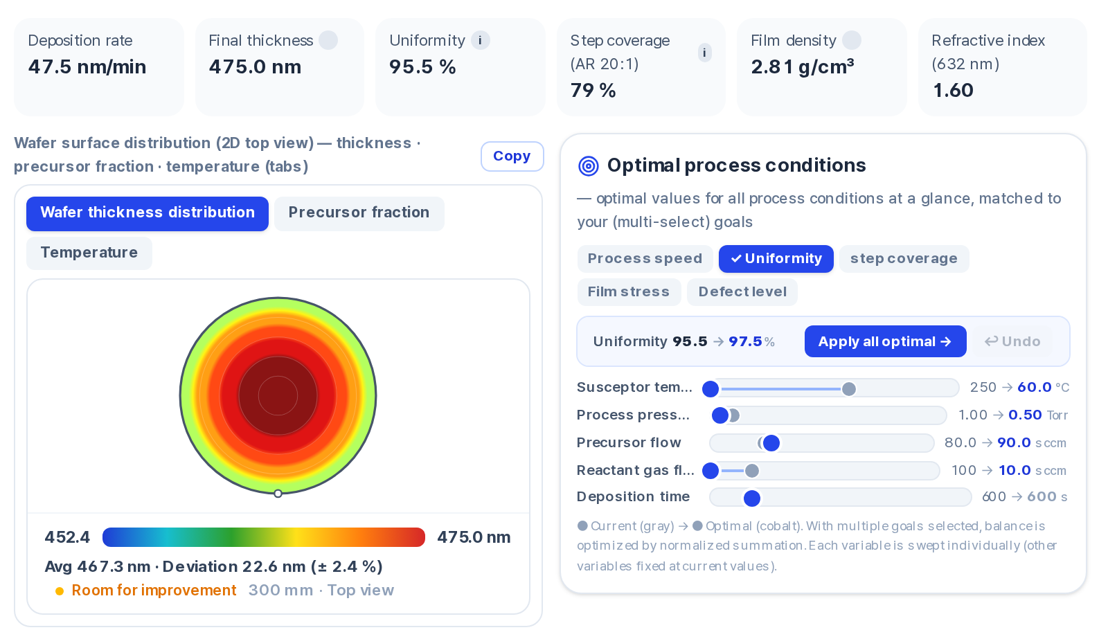
Semi Process Lab's CVD screen reports two uniformity numbers, and they are not interchangeable. The map caption reads Mean … deviation … (± X %), where the ± value is a half-range metric: (max − min) / (2 × mean) × 100. The headline Uniformity number uses a different formula: 100 − 1σ %, where σ is the standard-deviation spread. A higher headline number means tighter uniformity.
The grade system — Very uniform at or below 1 %, Room for improvement between 1 % and 2.5 %, Highly non-uniform above 2.5 % — applies to the caption's ± half-range value, not to the headline number. Mixing the two up can lead to the wrong conclusion. The two numbers measure different things.
What the Radial Map Is Good At
The screen accepts five inputs — temperature (susceptor or chamber), pressure, precursor flow, reactant gas flow (10–500 sccm, default 100 sccm), and deposition time (10–3600 s, default 600 s). When the PECVD process variant is selected, an RF power input appears as well.
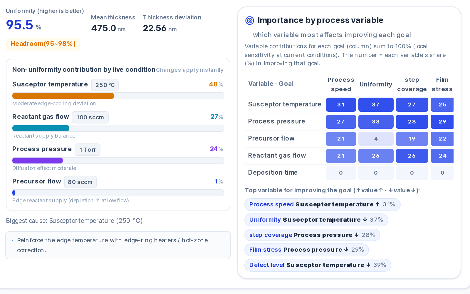
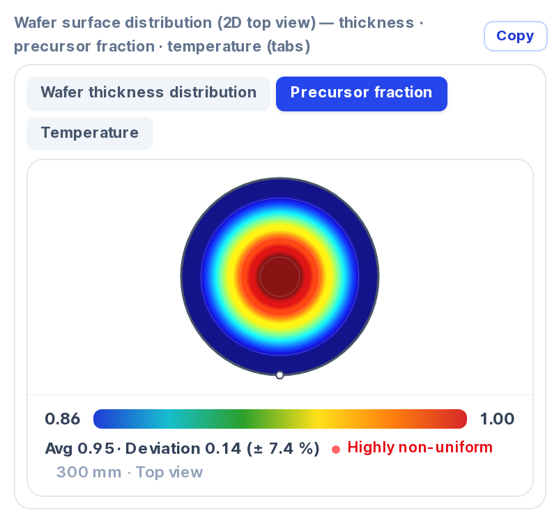
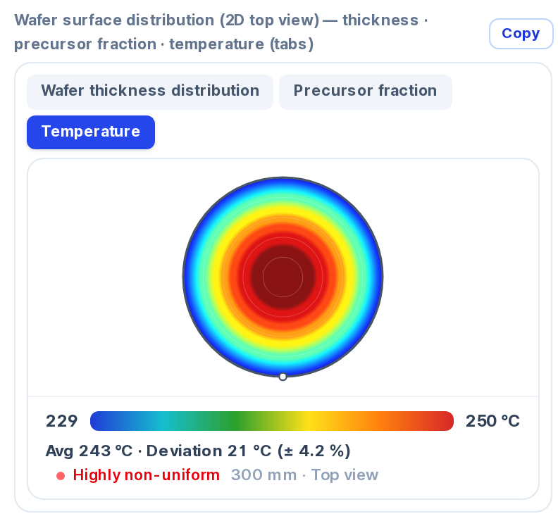
From those inputs the model returns a deposition rate in nm/min and a 300 mm wafer map with three selectable tabs: thickness, precursor fraction, and temperature. Each tab shows the radial distribution across the wafer. A contribution breakdown shows how much each process variable adds to the 1σ non-uniformity, benchmarked against a target of less than 2 %. A variable-importance ranking tells you which input has the largest leverage over thickness spread — helpful when you need to decide which knob deserves attention first.
For non-uniformity that varies with radius, the predicted map shows the modeled gradient and the panels show which process variable the model attributes it to.
Radial Versus Azimuthal
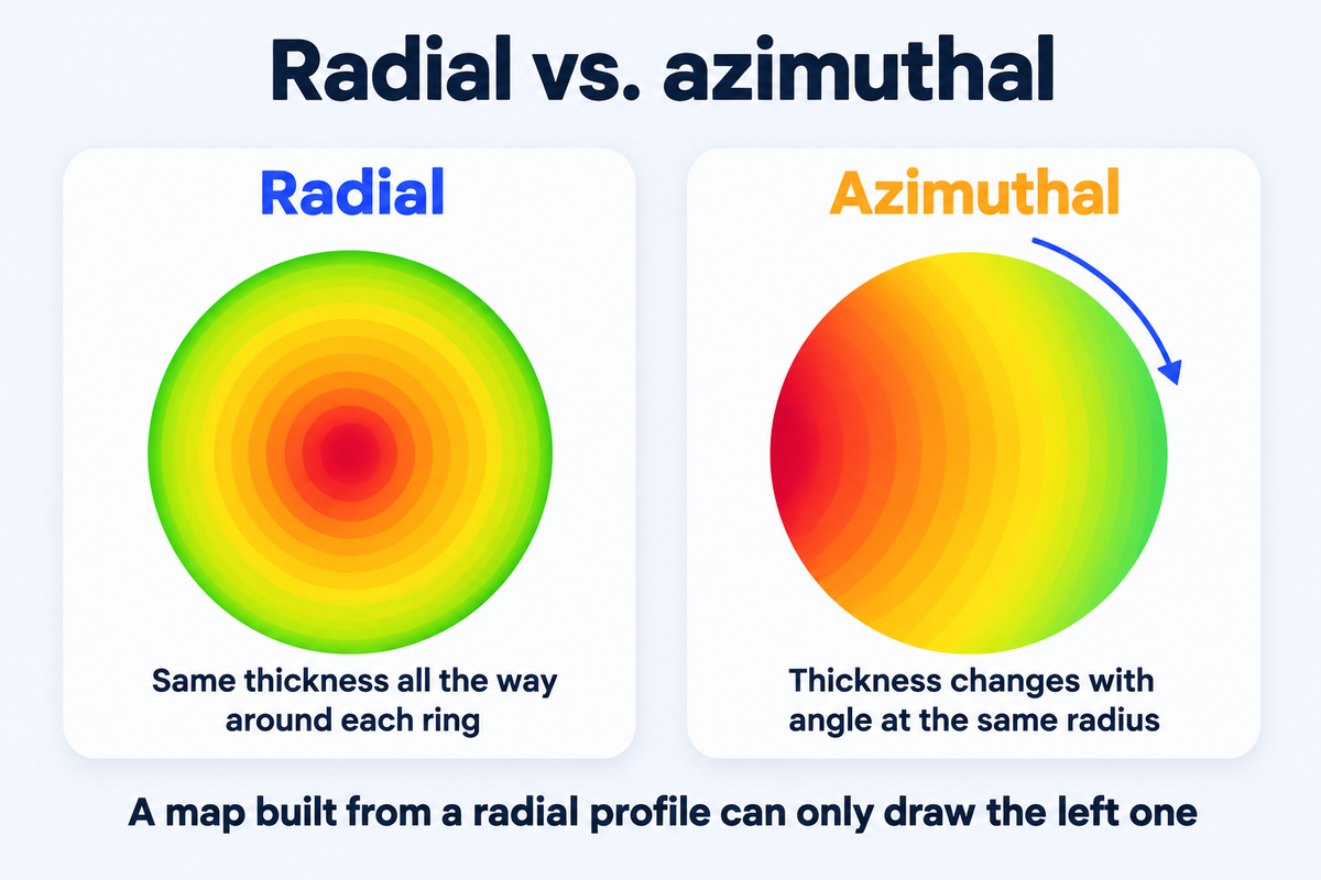
A radial pattern depends only on distance from the center. At any given radius the thickness is the same all the way around, forming a ring. An azimuthal pattern breaks that symmetry: thickness changes with angle at the same radius. One side of the wafer may be thicker than the other.
The distinction matters because a radial profile cannot express an azimuthal pattern. The product page names slot-valve asymmetry and pump-side tilt in its limits section, and pump-port tilt and a gas-inlet jet in its FAQ, as azimuthal effects the map does not capture.
The CVD screen's map is built from a radial profile. It renders concentric rings. Any thickness variation that depends on angle at a fixed radius is absent from the picture.
What It Cannot Show
The product page states the limits directly. The wafer map is radially symmetric and does not capture azimuthal effects such as slot-valve asymmetry or pump-side tilt. If your uniformity problem has a left-right or angular signature, the map will not reveal it.
The precursor-fraction and temperature tabs are derived from the input conditions using simplified relations, not a full transport calculation. They are not a substitute for measured profiles.
All results are design-reference estimates intended for comparing process directions. They are not a replacement for on-tool metrology. The screen predicts; the wafer confirms.
Analysing azimuthal patterns requires on-wafer measurement data. A map built from a radial profile cannot show them.
How to Use It Anyway
A radial map that knows its own limits is still a practical tool. The workflow is five steps:
- Open the Process design tab and click the CVD button. Plasma CVD is chosen through the gas selection.
- Set temperature, pressure, precursor flow, reactant gas flow, and deposition time with the sliders.
- Run the prediction to generate the wafer map and the uniformity grade.
- Switch between the thickness, precursor-fraction, and temperature tabs on the map to see where the radial spread originates.
- Read the contribution and importance panels to identify which variable to adjust first.
If the predicted radial non-uniformity already exceeds your budget, that is a radial direction you can explore here. Angular patterns on measured wafers fall outside what this map captures; that analysis needs on-wafer measurement data.
FAQ
What do the two uniformity numbers mean? The ± value in the map caption is a half-range metric: (max − min) / (2 × mean) × 100. The headline Uniformity number is 100 − 1σ %, where higher means tighter spread. The contribution panel uses the 1σ percentage, benchmarked against a less-than-2 % threshold. Always check which formula you are reading before comparing numbers across tools or reports.
Can the wafer map show left-right or slot-side asymmetry? No. The map is generated from a radial profile and renders concentric rings. It does not capture azimuthal patterns such as a pump-port tilt or gas-inlet jet. For that kind of analysis you would need on-wafer measurement data.
What does the importance panel tell me that the contribution panel does not? The contribution panel shows each variable's share of the total 1σ non-uniformity — how much of the current spread comes from temperature versus pressure versus flow. The importance panel ranks which input has the largest leverage over the spread, which helps you decide which knob to turn first.
Should I trust the predicted uniformity grade for a process-of-record decision? The grade is a design-reference estimate. It helps you compare directions — does raising pressure tighten or loosen the radial spread? — but it does not replace on-tool metrology. Use the prediction to narrow the search space, then confirm the result on actual wafers.
Semi Process Lab's CVD screen shows the wafer map, the contribution breakdown and the variable importance ranking for conditions you set. Every value on the screen is a model prediction for design reference, not a wafer measurement - use it to narrow the search, then confirm on silicon.