
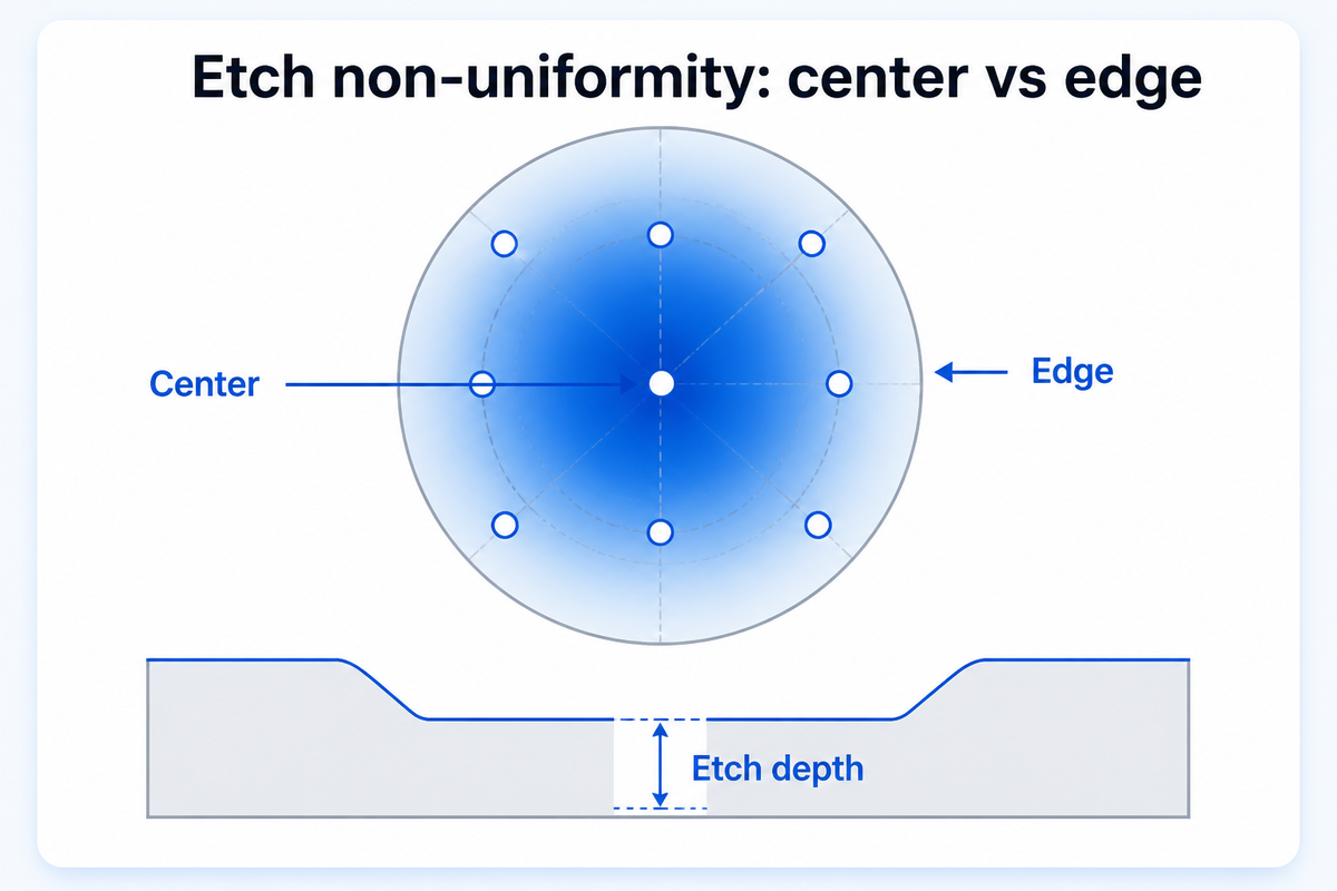
Etch non-uniformity is the variation in etch depth or rate across a wafer — center thicker than edge, one side faster than the other, or random pockets of under-etch. Pressure, gas delivery, power profile, pattern density, and edge effects all contribute. The instinct is to split wafers and change one knob at a time until the map improves. A faster starting point: find which variable dominates uniformity at your current operating conditions, adjust that one first, then confirm on wafers.
How Etch Non-Uniformity Is Reported
Two formulas are widely used. The range-based formula takes (max − min) / (2 × mean) × 100%. The standard-deviation formula takes 1σ / mean × 100%. Applied to the same wafer, they return different numbers — the range-based value is almost always larger because it is driven by the two most extreme points.
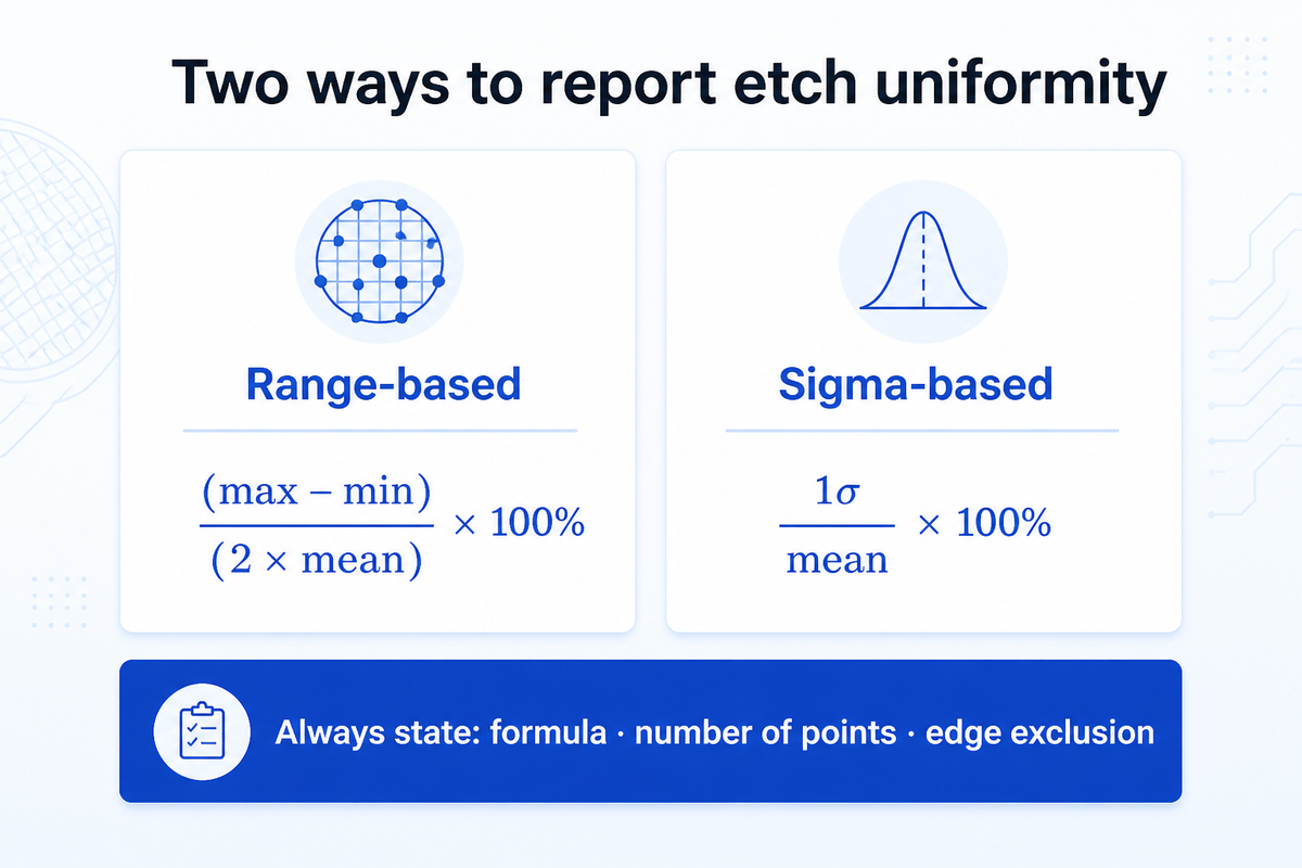
A uniformity percentage is only meaningful alongside three pieces of context: which formula was used, how many measurement points were taken, and what edge exclusion was applied. Edge exclusion matters more than most engineers expect. Points near the edge ring often etch at a different rate than the wafer interior, and including or excluding them can swing the reported value by a noticeable amount.
Where It Comes From
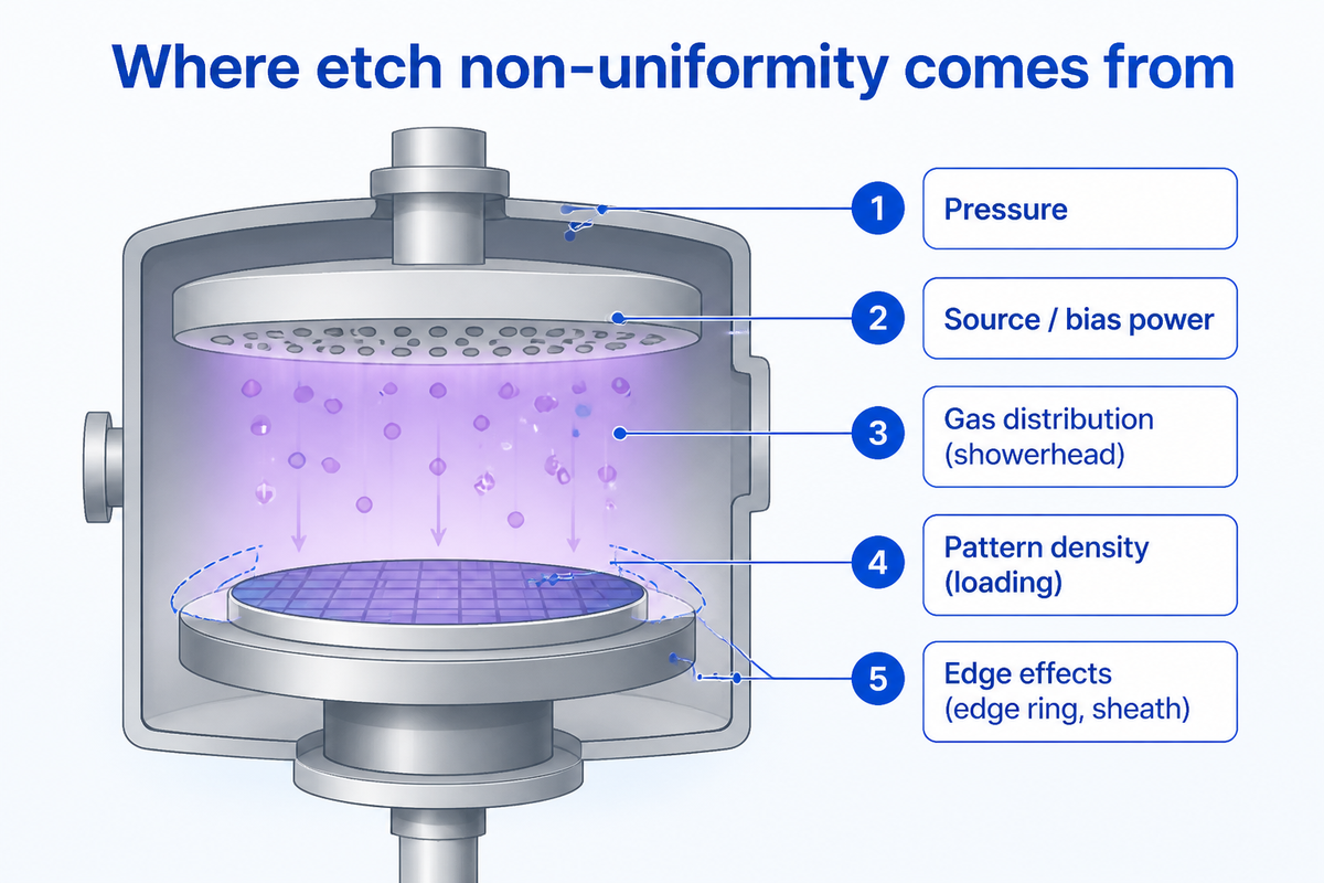
Chamber pressure gradients change radical and ion density from center to edge. Power distribution — both source and bias — shapes the ion energy and flux profile across the wafer. The showerhead determines where fresh gas arrives; any flow asymmetry appears directly in the etch map. Pattern density introduces loading and microloading: densely patterned areas consume etchant faster, locally starving adjacent regions. Edge effects from the edge ring geometry and sheath bowing create a distinct etch zone at the wafer perimeter. Temperature variation across the chuck shifts etch chemistry locally.
These causes overlap on every wafer. A single etch map cannot separate them cleanly, which is why blind one-at-a-time sweeps are expensive — you may be turning the wrong knob first.
Find the Dominant Knob at Your Current Conditions
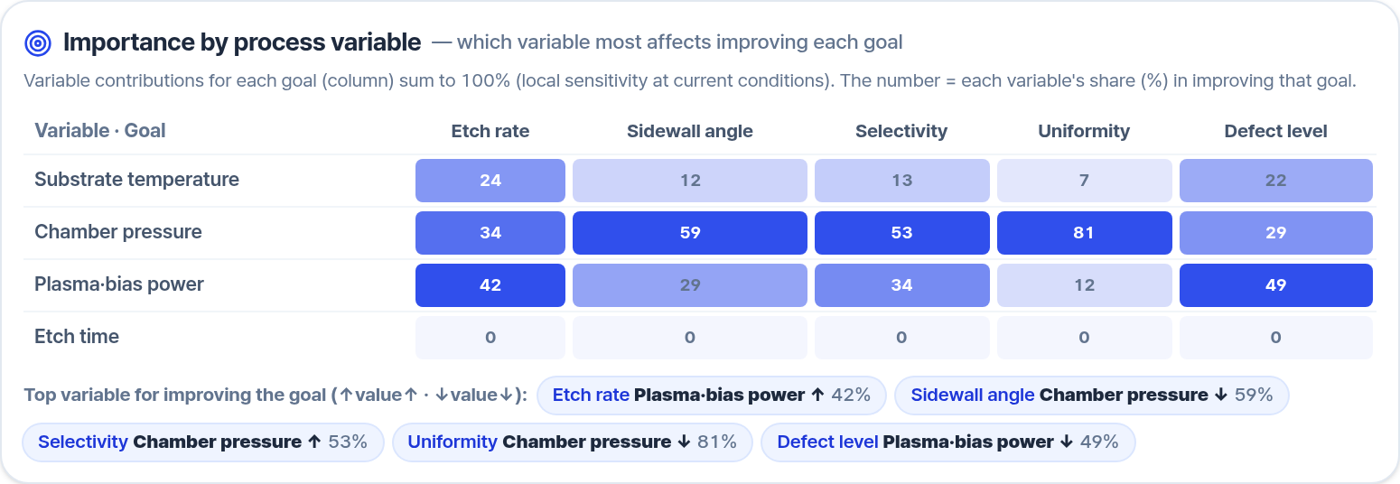
A sensitivity breakdown at your current conditions tells you where to look first. In this example — Al₂O₃ reactive-ion etch with BCl₃/O₂/Ar at 30 mTorr, 300 W, and 250 °C — chamber pressure accounts for 81% of the uniformity sensitivity. Plasma and bias power contribute 12%, substrate temperature 7%, etch time nearly zero. The direction flag indicates that lowering pressure improves uniformity at this operating point.
This is a local sensitivity: it ranks the knobs near where you are right now. If you move to a substantially different pressure regime, the ranking could shift. That is expected — sensitivity depends on where you sit in the process space, not on a fixed property of the chamber.
What the Model Suggests — and What It Does Not
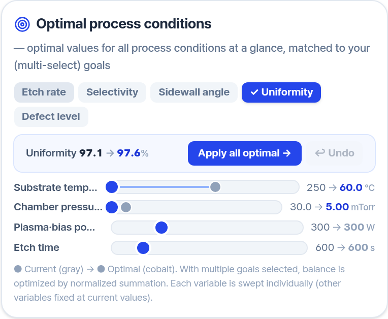
Sweeping each variable one at a time while holding the others fixed, the model predicts uniformity moves from 97.1% to 97.6% by dropping chamber pressure from 30 to 5 mTorr and substrate temperature from 250 to 60 °C. Power and etch time stay unchanged — the model finds no gain from adjusting them at this point.
Two limits matter. First, each variable is swept independently, so interactions — pressure × power, for example — are not captured. A change that helps in a single-variable sweep may behave differently when two knobs move together. Second, every number here is a rule-based model prediction, not a wafer measurement. The model points a direction. The wafer confirms it.
Confirm on Wafers
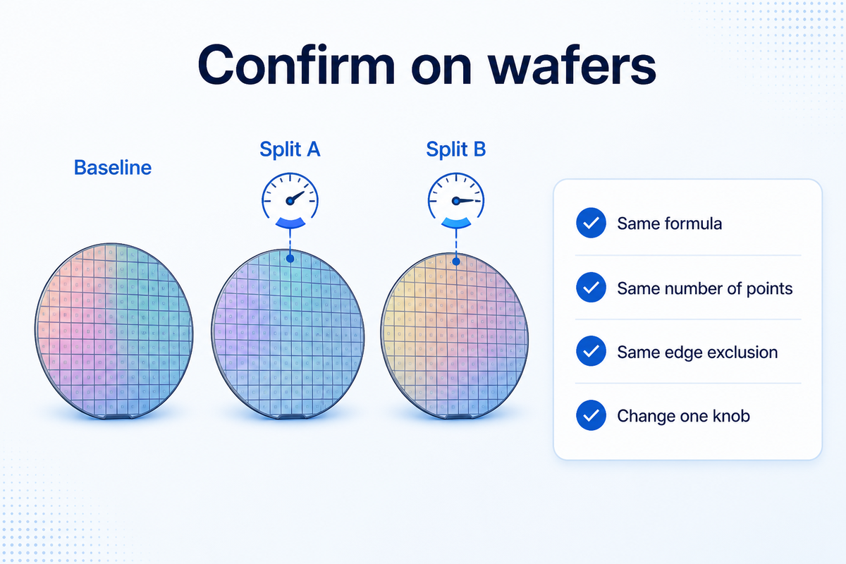
Model output narrows your search. Wafers close the loop. When you run confirmation splits, match the baseline measurement setup exactly: same uniformity formula, same number of measurement points, same edge exclusion. Changing any of these between baseline and experiment means you are comparing different numbers, not different processes.
Keep the splits focused. If sensitivity says pressure dominates at 81%, your first split is a pressure variation — not a full factorial across every variable. One knob, a handful of wafers, a clean comparison.
FAQ
What is a good etch uniformity?
It depends on the process and the device. A blanket film strip and a patterned gate etch tolerate different spreads. The threshold is set by what the downstream integration step requires, not by a universal number.
How do you calculate etch uniformity?
Two common formulas: (max − min) / (2 × mean) × 100%, and 1σ / mean × 100%. They give different values on identical data. Always report which formula, how many measurement points, and what edge exclusion was applied.
Why is my etch faster at the edge?
Typical causes include higher radical flux at the wafer edge from gas flow geometry, lower local pattern density reducing loading, and edge ring or sheath geometry concentrating ion flux outward. The dominant cause depends on the chamber and recipe.
Does lower pressure always improve uniformity?
Not necessarily. In the model behind the screens above, non-uniformity rises at high pressure as the radical distribution worsens, but it also rises again below about 2 mTorr, where local etch differences grow. The relationship is not monotonic. Confirm the direction in your own chamber before locking in a target.
Semi Process Lab's process design screen shows per-variable sensitivity and single-variable optimization for etch uniformity, so you can identify the dominant knob before committing to wafer splits. Every value on the screen is a rule-based model prediction, not a wafer measurement — use it to narrow the search, then verify on silicon. Semi Process Lab