
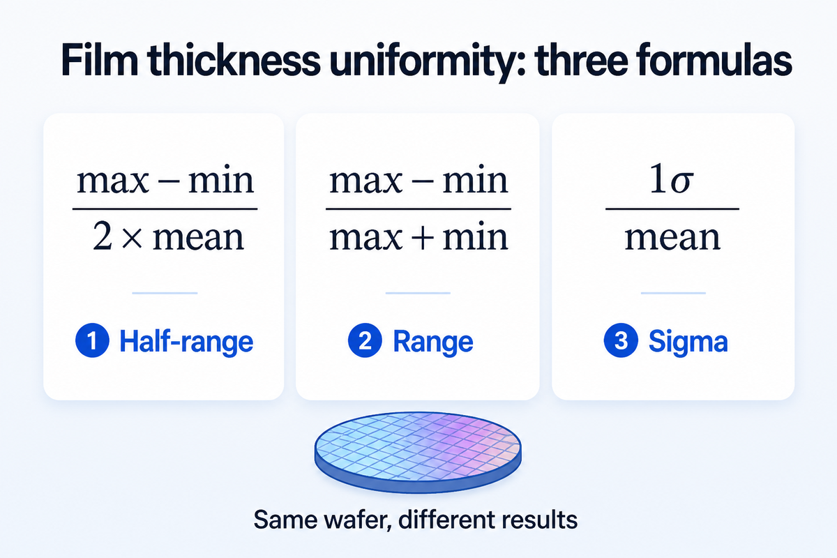
Every semiconductor and display fab tracks film thickness uniformity, yet the single percentage on a metrology report can come from at least three different formulas. Half-range calculates (max − min) / (2 × mean) × 100 % and is written as ± %. Range uses (max − min) / (max + min) × 100 %. Sigma takes 1σ / mean × 100 %, sometimes reported as 3σ. Apply all three to the same wafer and you get three different numbers.
The Three Formulas and What Each One Hears
Half-range divides the full spread by twice the mean, then expresses the result as ± %. It is a common way to state a spread as a ± value. Because it uses only the maximum and minimum thickness, a single outlier point—at the center or at the edge—moves the number.
Range divides (max − min) by (max + min). The denominator is close to 2 × mean when uniformity is good, so range and half-range give nearly identical values for uniform films. They diverge when the spread is large relative to the mean.
Sigma (1σ / mean) uses every measured point to compute a standard deviation, then normalizes by the mean. It is less sensitive to a single extreme point because every point contributes equally to the variance. Some fabs report 3σ / mean instead; the choice is convention, not physics.
Range-based formulas react to extremes. If one edge site is anomalously thin, both half-range and range jump, while sigma moves less. Neither approach is wrong. They answer slightly different questions: "How far apart are the worst points?" versus "How spread out is the entire distribution?"
Same Map, Different Numbers
A concrete example makes the difference visible. The map below is a model prediction for ALD Al₂O₃ under problem conditions on a 300 mm wafer. The center is thick and the edge is thin.
The legend reads Avg 26.5 nm · Deviation 8.2 nm (± 15.4 %). Here, Deviation is the range (max − min) and the ± % is the half-range formula: (max − min) / (2 × mean). These values are model predictions, not physical wafer measurements.
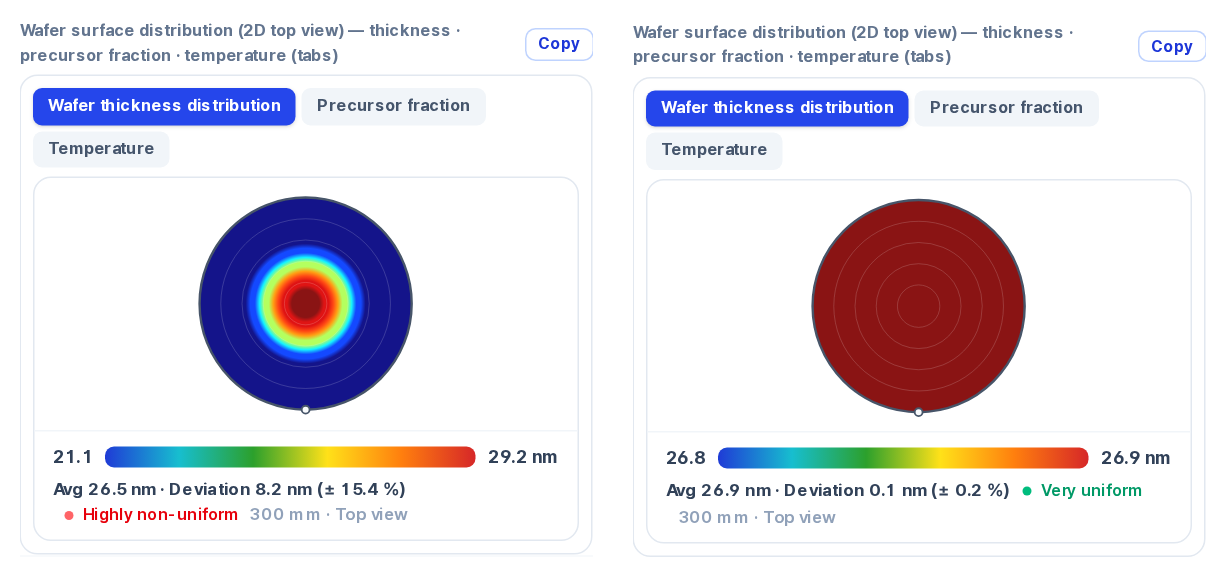
Under standard conditions, the same film shows Avg 26.9 nm · Deviation 0.1 nm (± 0.2 %). Again, a model prediction.
If you applied 1σ / mean to either map, you would get a different percentage—not because the film changed, but because the formula changed.
Where You Measure Changes the Answer
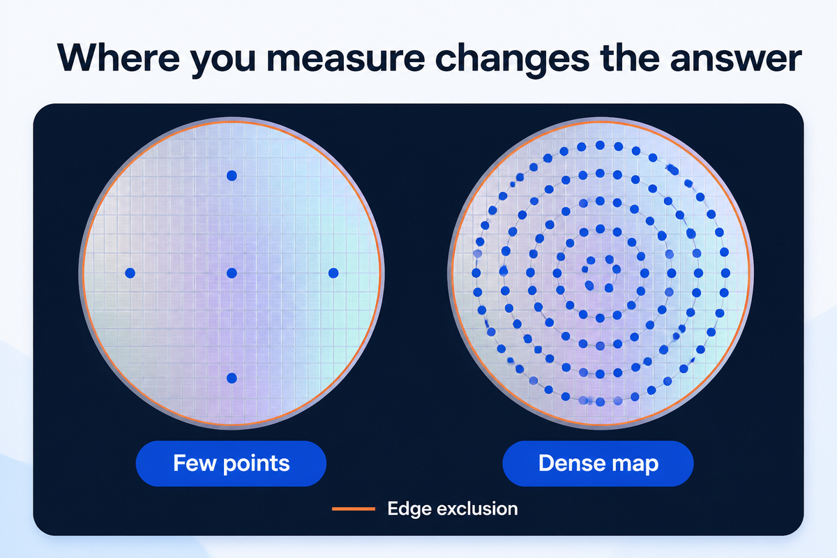
The measurement pattern shapes the result as much as the formula does. A 5-point pattern may miss a center peak entirely. A 49-point concentric-ring map captures it. A sparse pattern that skips the edge can report good uniformity even when edge roll-off is severe.
Edge exclusion matters just as much. The outer few millimeters of a wafer often show a thickness rise or drop. Changing the exclusion width can shift the reported number substantially, because you are adding or removing the points most likely to be extreme.
Within-Wafer vs Wafer-to-Wafer
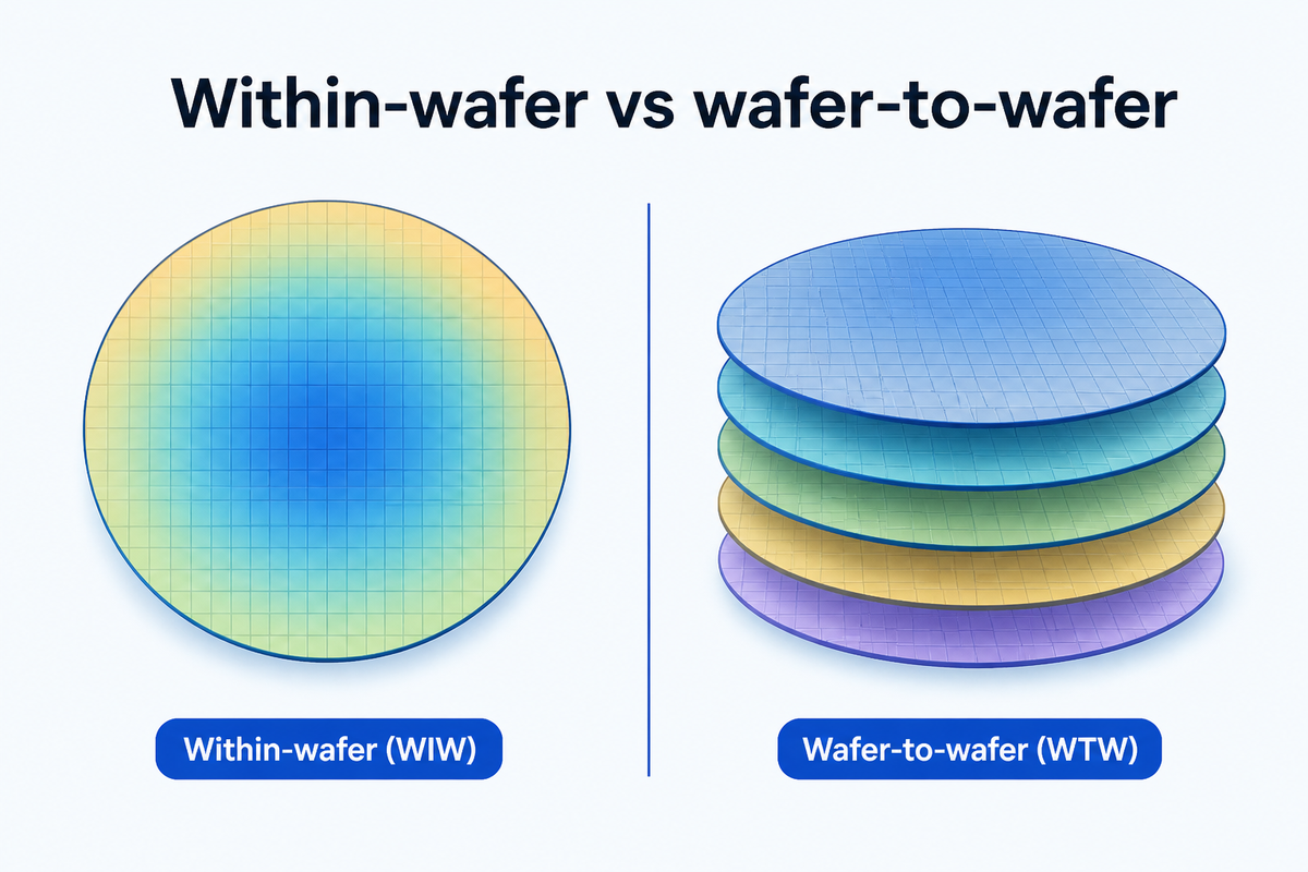
Within-wafer (WIW) uniformity describes how thickness varies across a single wafer. Wafer-to-wafer (WTW) uniformity compares wafer means across a lot or across runs. A process can have tight WIW uniformity but drift run to run, or the reverse. Both matter, but they answer different questions and should not be mixed in the same column of a table.
How to Report It
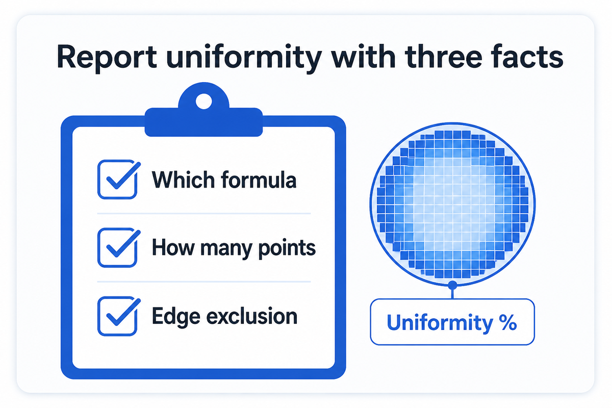
A uniformity percentage is not comparable unless you state three facts: which formula you used, how many points you measured (and in what pattern), and what edge exclusion you applied. Some tools print uniformity and others print non-uniformity (100 % minus the other), so say which one the number is. Specify WIW or WTW. Without these details, a number from one tool cannot be compared to a number from another.
FAQ
What is the formula for thickness uniformity?
There is no single formula. The three most common are half-range (max − min) / (2 × mean) × 100 %, range (max − min) / (max + min) × 100 %, and sigma 1σ / mean × 100 %. Each gives a different percentage from the same data. Check which one your tool or spec uses before comparing numbers.
Is 1σ or range better?
Neither is inherently better. Range-based formulas are driven by the two most extreme points, so they flag worst-case spread. Sigma uses every point, so it is more stable against a single outlier. Many fabs use both and look at them together.
Why does my uniformity change when edge exclusion changes?
Film thickness often rolls off or rises near the wafer edge. Including or excluding those outer millimeters adds or removes the points most likely to be the maximum or minimum. That shifts range-based formulas directly and changes the standard deviation as well.
What is a good uniformity value?
It depends on the film, the layer's function, and the downstream process tolerance. A number that is acceptable for one application may not be for another. Report the context—film type, formula, point count, edge exclusion—so the number can be judged against the right requirement.
Semi Process Lab's process design screen is built to use one statistic convention across its views, so the same film is not reported two ways. The wafer map legend shows the half-range formula as ± % and the full range as Deviation. The values are model predictions meant to narrow the process search before you run wafers. Once you have a promising condition, verify it on real wafers with your own metrology. Try it at Semi Process Lab.