
A semiconductor device cross section is the labeled side view of a transistor, memory cell, sensor or display backplane device — every film from the substrate up, with its material and thickness. Semiconductor and display engineers put one in almost every talk, paper and design review, because it answers "what is this device made of?" in one picture. A good one shows five things: layer order, material names, thickness with units, dimension lines and a note on scale.
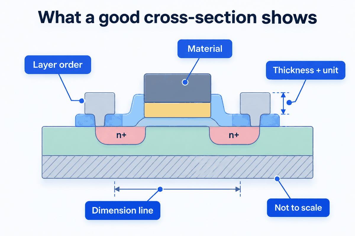
What a good semiconductor device cross section shows
Layer order. Films appear top to bottom in the order they sit on the wafer. A stray swap — the dielectric drawn above the gate metal — is the first thing a reviewer catches.
Material and thickness. Each film carries its material (HfO₂, TiN, SiO₂ …) and a thickness with its unit. Nanometres for gate stacks, micrometres for thick layers; never a bare number.
Dimension lines and a scale note. Lateral sizes such as fin width or pitch get a dimension line. Then say whether the drawing is to scale — most are not, and that is fine as long as you say so.
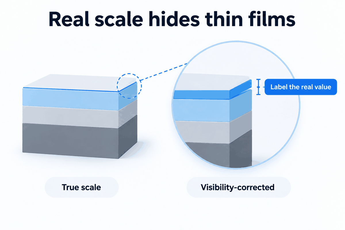
Real scale hides thin films
Draw a gate stack at true scale and a 2 nm dielectric on a 50 nm substrate becomes a hairline you cannot see, let alone label. That is why most device figures are drawn with visibility-corrected proportions: thin films are drawn thicker than their true ratio so every layer stays readable.
The rule that keeps this honest is simple — the picture is for reading, the label is for the value. Write "2 nm" on the film, and state "not to scale" in the figure or caption.
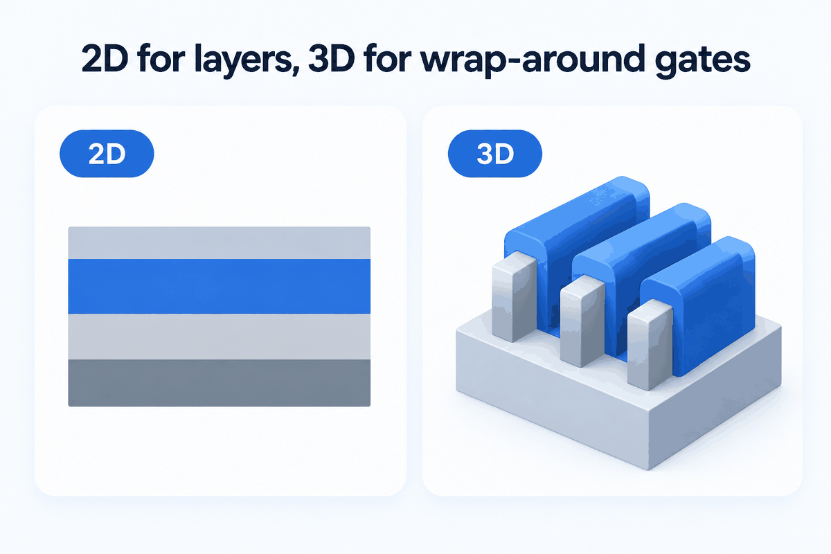
2D for layers, 3D for wrap-around gates
A 2D section is the clearest way to show a planar stack — a planar MOSFET, a MOS capacitor, a thin-film transistor, a solar-cell stack. Order and thickness read instantly.
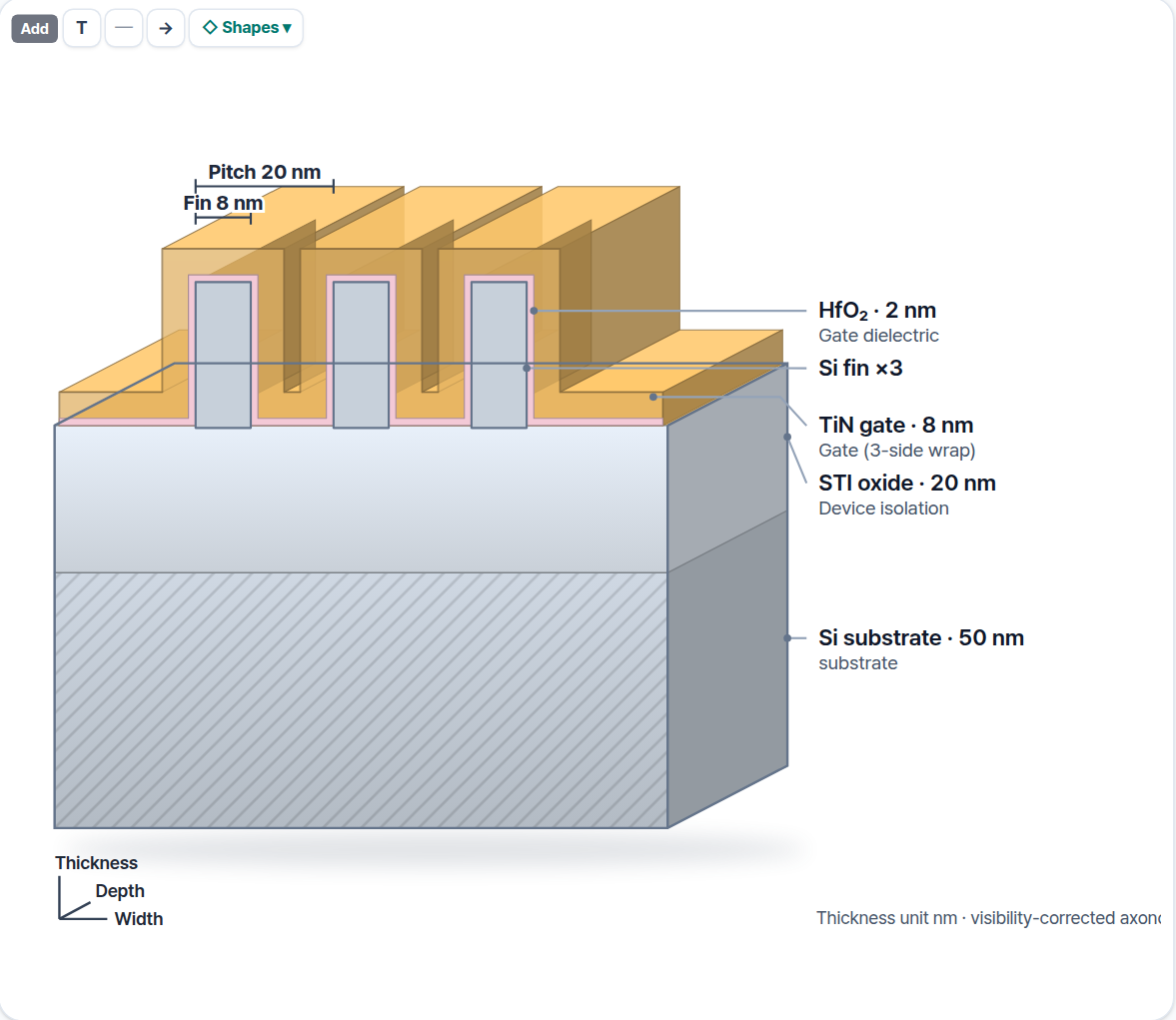
Once the gate wraps the channel, 2D starts to hide the point. A FinFET gate covers three sides of each fin; a GAA nanosheet gate surrounds each sheet. A 3D view with width, depth and thickness axes shows that wrap in one look.
Start from a template instead of rectangles
Most of us build these in a slide tool, one rectangle at a time, and redraw everything when a thickness changes. In Semi Process Lab, the Design Studio starts you from a template instead. Under Device Cross-section there are ready structures — Planar MOSFET, FinFET, GAA nanosheet, GaN HEMT, IGZO TFT, FeFET, Perovskite solar and more — next to Deposition Stack, Etch Structure and Chamber · Equipment groups.
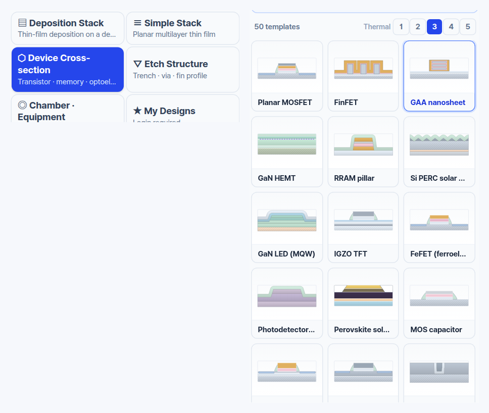
Pick one and the section appears with every film labelled with its material and thickness, plus dimension lines. Click a layer label to select it, then drag to change thickness or width; the Layer composition (top→bottom) table lists each film, with + Layer and + Pair ×N for repeated stacks. The values in a template are starting examples — replace them with yours. The screen notes that thickness is in nm and the drawing ratio is visibility-corrected.
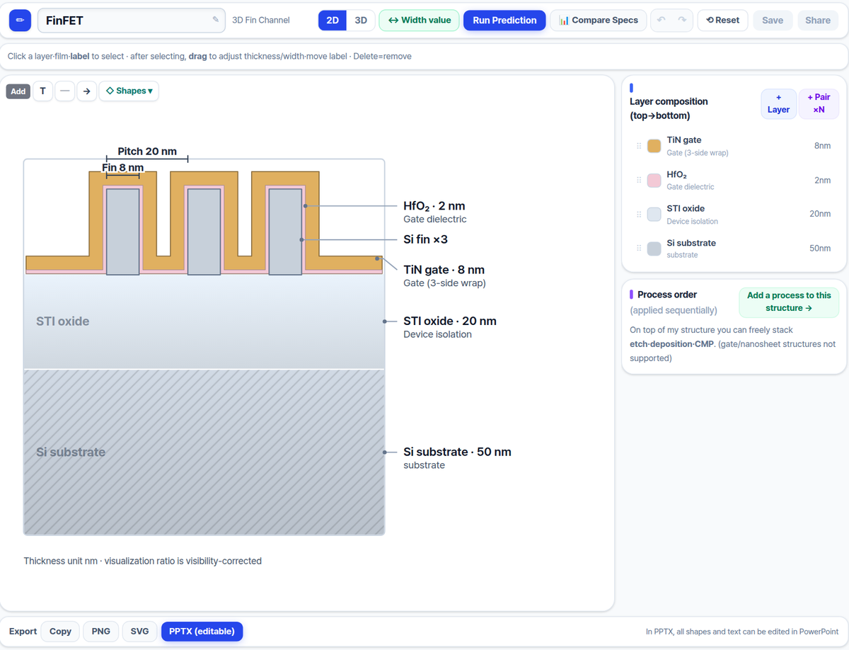
Switch 2D / 3D to see the same structure in 3D with thickness, depth and width axes. When it is done, Export as PNG, SVG or PPTX (editable) — in the PPTX every shape and text stays editable in PowerPoint, so a last-minute thickness change does not mean a redraw. From the same screen, Run Prediction takes the structure into Design & Predict.
FAQ
What should a semiconductor device cross section include?
Every film that matters to your point, in the right top-to-bottom order, each with its material name and a thickness with units. Add dimension lines for lateral sizes and a note saying whether the drawing is to scale.
Should a device cross section be drawn to scale?
Usually not. At true scale a nanometre-thin film disappears next to the substrate. Draw thin films larger so they stay readable, keep the real thickness in the label and mark the figure "not to scale".
When is a 3D view better than 2D?
When the gate or contact wraps the channel — FinFETs, GAA nanosheets, trench structures. For planar stacks, 2D is faster to read.
How do I keep a cross section editable for later changes?
Keep it as editable shapes rather than a flat image. Exporting to an editable PPTX lets you change a thickness or a label later without redrawing the figure.